Death by a Thousand Opcodes
A mod (jokingly) told me I had to make a Neo Geo Pocket emulator, so I intend to showcase the pain that has caused me. This was going to be a list of rants, but most of them were way too short, so enjoy this diary of things that made me go WTF instead.
10/18/2023 - Register Encoding
I started work on this emulator recently. The TLCS-900/H is a really cool processor, but I want to personally murder whoever made the register encoding. My first encounter with it was this:


Seems OK enough. 8 32-bit registers, 8 16-bit registers, and 8 8-bit registers structured in a way reminiscent of SM83, 8080, Z80, etc. It’s familiar to me and shouldn’t be a problem. The main 4 are banked (controlled by some bits in SR) and the other 4 are always the same, but that’s fine. I’ve done that before too. After ARM, I’m not scared of a beefed-up Game Boy. At least SR, F, and PC aren’t GPRs. Scrolling down some more…
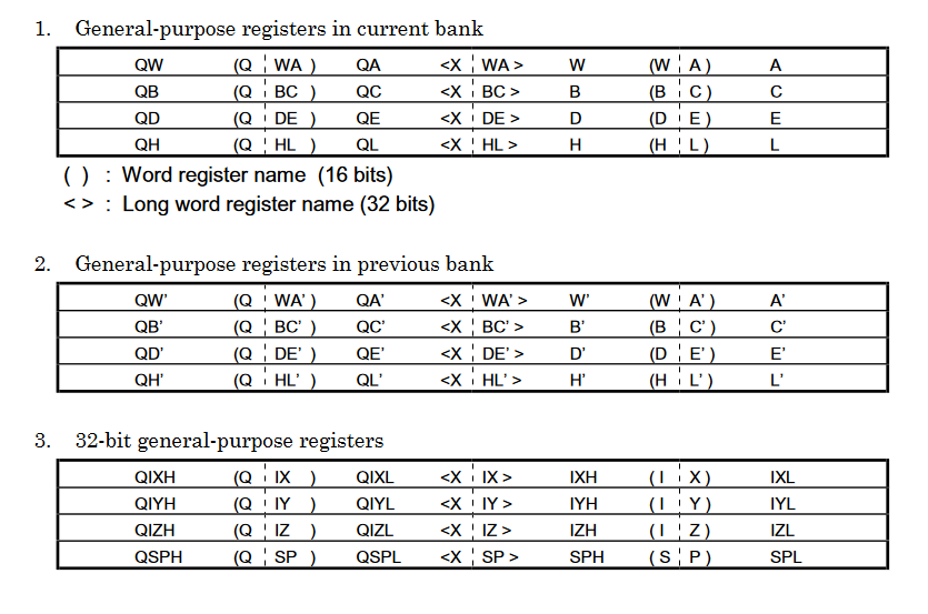
spends 20 minutes figuring out how to read the table Q registers? Ok, so pointer math is definitely the way to index these. Otherwise it’s just a confirmation of what I already know. I do wonder why included the 8-bit segments of WIX/WIY/WIZ/WSP because the last diagram said you couldn’t use them. Eh, probably for consistency. Also weird that they felt the need to give names to the previous bank’s registers.

Sure, I see how you’d need a way to talk about a register in any bank. The interrupt chapter I skipped does seem talk a lot about the state in multiple banks at the same time. These naming schemes are getting increasingly nonsensical though.

That explains the Q register thing. I’ll be sure to keep an eye out for that prefix byte. Time to figure out the encoding.

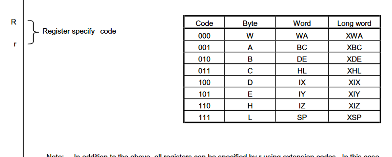
Maybe it was all a bad dream. All I have to worry about is my simple 3 groups of 8. Hey, what’s that thing down there?

Uhhh….

😢 🔫
waityoumeanyoucanaccessanybyteofanyregisteratanytime whatsthepointofthosediagramsatthebeginning theres196possibleregisters whydidyouonlylisttwentyfourpossibilitiesacouplepagesearlier doihavetousethistableandcontextfromtheinstructionsoperandsizetoknowwhichregisteritmeans ifyouregoingtogowithagiantstupideightbittableyoucouldatleastmakeeachpossibilityitsownentry betteryetstoppretendingyoureriscandaddmandatorymodrmbyteseverywherelikex86 youhaveoddlyspecificinstructionsthatdontevenexistinmodernprocessorsandtheonlythingyouhaveincommonwiththez80youclaimtobeadecentantofisregisternameswhichyoustillmanagedtomessupinanhonestlyimpressiveway thatwayyoucanusewhateverwierdregisterencodingyouwantdropthelimitationof8registersandputitallsomewherepeopleexpectitinsteadofmakinghalftheinstructionspaceprefixbytesthatunlockbasicaddressingmodes
10/19/2023 - Addressing Modes
Part 1
It took me days of staring at the CPU manual and the Ghidra disassembly of an instruction, but I finally figured out how prefix bytes work. In the main opcode table (which uses different operand syntax than the rest of the document for some reason), there are 115 bytes dedicated to prefixes. Each of these bytes can do up to 3 things:
- Set a source, destination, or register addressing mode. The source and destination prefixes encode 22 addressing modes that fit into 9 categories. Some of these addressing modes require extra data that’s stored in the following bytes. The register prefixes can either select 1 of 8 general purpose registers or be followed by an extra byte that should be very familiar to you by now.
- Choose the opcode table. After the addressing mode byte(s) is the actual opcode. Source, destination, and register modifications each
- Choose the size of the operands. The source and register prefixes can also choose whether the actual instruction operates on a Byte, Word, or Long. Some of the instructions in the secondary table only work with one or two sizes, so I have no idea what happens when I mismatch them.
I don’t know whether this is a horrible and unnecessarily complicated encoding or genius, and at this point I don’t care. All I do know is I’m thankful that you can only use one of them per instruction.
Part 2
I just found out you can use pre-decrement/post-increment addressing modes in RMW instructions or as the destination, and there aren’t enough examples in the manual to answer my question. I know the destination address is fetched before the instruction is executed in absolute mode, but I don’t know when it’s calculated and when/if it gets latched for the indirect modes. Like what would happen if I did LD XWA, (-XWA), LD XWA, (XWA+), or LD (-XWA), XWA? Actually, I’m not even sure about LD (XWA+), XWA. Maybe there’ll be some hints in the timing stuff I skipped over? I doubt it would be nearly as detailed as the ARM7TDMI’s.
10/21/2023
I’m still very early in the BIOS. Implementing instructions as I run into them, looking at the execution log, and contemplating whether I should make a commented Ghidra disassembly. As someone who was too scared to implement registers until yesterday, I should not be better at this CPU than the programmers at SNK.
For context, all the addresses it’s writing are in WRAM. I don’t know why they choose to spend two instructions writing one-byte values to adjacent addresses when they could save 4 bytes by storing a word instead, especially when they’ve shown they know how. My only guess is the function was written in C and they used a crappy compiler.
10/26/2023
I’ve been making a little progress. For the source prefix addressing modes, I decided to choose the behavior that made the most sense to me and go with it, but then I discovered something weirder. Despite being in the source addressing mode table, there are many opcodes that use the computed address for the destination. Looking at the destination opcode table, I noticed a lot of the instructions were about single-bits and the carry flag. Maybe source and destination are inaccurate names for the tables/prefixes?
It’d probably be best to have asserts everywhere that warn me when the same register gets used in the address and operand, but that seems like a lot of work. I think I did find a clean-ish way to handle the different operand sizes though. I split the 3 prefix opcode tables into their own functions and templated the source/register ones based on size. That way I can treat certain instructions the same no matter the size, throw an error when instructions are used with the wrong size, and make different versions of/slight modifications to some instructions based on size. I also made templated versions of common instructions that show up in a few places (AND, OR, PUSH, etc.), so I can often use the same code for multiple sizes by passing the size template parameter to that. Like reg32[opcode & 7] = OR<T>(operand1, operand2); instead of making a branch that calls OR<u8>(), a branch that calls OR<u16>(), and a branch that calls OR<u32>().
Back to why I started writing this before going on a tangent about source prefixes. I ran into one of the last things I wanted to see today: F5 F2 65 a.k.a. LD (XIX+), XIY. It has post-increment, destination addressing, and the dumb register byte all in one. What’s more, it uses a special version of the register byte where the bottom 2 bits instead choose how much the post-increment adds.